- 您现在的位置:买卖IC网 > Sheet目录2006 > LTC2704IGW-16#PBF (Linear Technology)IC DAC 16BIT QUAD VOUT 44-SSOP
LTC2704
18
2704fd
Voltage Output/Feedback and Compensation
TheLTC2704providesseparatevoltageoutputandfeedback
pins for each DAC. This allows compensation for resistance
between the output and load, or a current boosting stage
such as an LT1970 may be inserted without affecting ac-
curacy. When OUTx is connected directly to RFBx and no
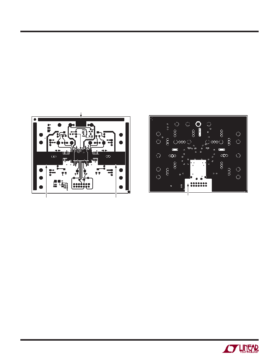
GND1 TRACE,
SEPARATED FROM
AGND UNDER LTC2704
EXPOSED GROUND PLANE AROUND EDGE
ALLOWS GROUNDING TO PROTOTYPE CIRCUITS
2704 F03
GND2 TRACE,
SEPARATED FROM
AGND UNDER LTC2704
CUTOUT PREVENTS DIGITAL RETURN CURRENTS
FROM COUPLING INTO ANALOG GROUND PLANE. NOTE
THAT THERE IS A PLANE IN THIS REGION ON LAYER 3
2704 F04
Figure 3. DC752 Top Layer
Figure 4. DC752 Analog Ground Layer. No Currents Are Returned
to this Plane, so it May Be Used As a Reference Point for Precise
Voltage Measurements
additional capacitance is present, the internal frequency
compensation is sufcient for stability and is optimized
for fast settling time. If a low bandwidth booster stage is
used, then a compensation capacitor from OUTx to C1x
may be required. Similarly, extra compensation may be
required to drive a heavy capacitive load.
APPLICATIONS INFORMATION
发布紧急采购,3分钟左右您将得到回复。
相关PDF资料
LTC2751AIUHF-16#PBF
IC DAC 16BIT CUR OUT 38-QFN
LTC2752ACLX#PBF
IC DAC 16BIT DUAL CUR OUT 48LQFP
LTC2753AIUK-16#TRPBF
IC DAC 16BIT DUAL 48-QFN
LTC2754AIUKG-16#PBF
IC DAC 16BIT QUAD IOUT 52-QFN
LTC2755AIUP-16#PBF
IC DAC 16BIT CUR OUT 64-QFN
LTC2757ACLX#PBF
IC DAC 18BIT PAR 48LQFP
LTC2758AILX#PBF
IC DAC 18BIT SPI/SRL 48-LQFP
LTC2844IG#TRPBF
IC TXRX 3.3V MULTIPROTCOL 28SSOP
相关代理商/技术参数
LTC2704IGW-16#TRPBF
功能描述:IC DAC 16BIT QUAD VOUT 44-SSOP RoHS:是 类别:集成电路 (IC) >> 数据采集 - 数模转换器 系列:- 标准包装:2,400 系列:- 设置时间:- 位数:18 数据接口:串行 转换器数目:3 电压电源:模拟和数字 功率耗散(最大):- 工作温度:-40°C ~ 85°C 安装类型:表面贴装 封装/外壳:36-TFBGA 供应商设备封装:36-TFBGA 包装:带卷 (TR) 输出数目和类型:* 采样率(每秒):*
LTC2713CM-G
制造商:Lite-On Semiconductor Corporation 功能描述:
LTC-2721B
功能描述:LED 显示器和配件 Blue 3 Dig 0.28" Ht 466nm 3000ucd RoHS:否 制造商:Avago Technologies 显示器类型:7 Segment 数位数量:2 字符大小:7.8 mm x 14.22 mm 照明颜色:Red 波长:628 nm 共用管脚:Common Anode 工作电压:2.05 V 工作电流:20 mA 最大工作温度:+ 85 C 最小工作温度:- 35 C 封装:Tube
LTC-2721E
功能描述:LED 显示器和配件 3 Digit, Orange RoHS:否 制造商:Avago Technologies 显示器类型:7 Segment 数位数量:2 字符大小:7.8 mm x 14.22 mm 照明颜色:Red 波长:628 nm 共用管脚:Common Anode 工作电压:2.05 V 工作电流:20 mA 最大工作温度:+ 85 C 最小工作温度:- 35 C 封装:Tube
LTC2721G
制造商:Lite-On Semiconductor Corporation 功能描述:
LTC-2721G
功能描述:LED 显示器和配件 3 Digit, Green RoHS:否 制造商:Avago Technologies 显示器类型:7 Segment 数位数量:2 字符大小:7.8 mm x 14.22 mm 照明颜色:Red 波长:628 nm 共用管脚:Common Anode 工作电压:2.05 V 工作电流:20 mA 最大工作温度:+ 85 C 最小工作温度:- 35 C 封装:Tube
LTC-2721JD
功能描述:LED 显示器和配件 3 Digit, Red Low Current RoHS:否 制造商:Avago Technologies 显示器类型:7 Segment 数位数量:2 字符大小:7.8 mm x 14.22 mm 照明颜色:Red 波长:628 nm 共用管脚:Common Anode 工作电压:2.05 V 工作电流:20 mA 最大工作温度:+ 85 C 最小工作温度:- 35 C 封装:Tube
LTC-2721KF-06
制造商:Lite-On Semiconductor Corporation 功能描述:DISPLAY,CLOCK - Bulk